|
|
Department
of Electrical and Computer Engineering Phone (850) 410-6220 Fax (850) 410-6479 Professor Dr. Uwe Meyer-Baese email: umb@eng.fsu.edu |
|
|
|


FROM: Dr.
U. Meyer-Baese
DATE:
SUBJECT: A/D
and D/A Nexys demo
ACKNOLEGMENT: This material is based upon work
supported by the National Science Foundation under Grant No. DUE-0442600."
Movie text: Welcome to a short demonstration of the D/A and A/D conversion using Digilent’s Nexys board. My name is Dr. Meyer-Baese. We use the MatLab/Simulink software and Xilinx System Generator to generate the VHDL code. Then we use the pin file (*.UCF) and Xilinx ISE to generate the bit stream. In the next step we then program the board via parallel cable using Xilinx IMPACT software or with the USB cable using Digilent ADEPT tools.
The test
circuit generated a sine and a triangular function using an accumulator and a
sine table. The D/A daughter board is connected to the
6-pin port JA and the A/D daughter board is connected to the port JD. The first
D/A channel shows a sine wave, while the second D/A
channel generates a slow triangular function. This triangular function is used
as input for the A/D converter and the output of the A/D conversion is shown on
the row of single LEDs. We can change the frequency of the signals using the 8
switches on the Nexys board. The 4 buttons are used
as enable for the 7 segment elements. In addition button 0 is used as reset and
button 3 is used to display the second input A/D channel. This concludes the
demonstration of the A/D and D/A conversion using Digilent Nexys
boards
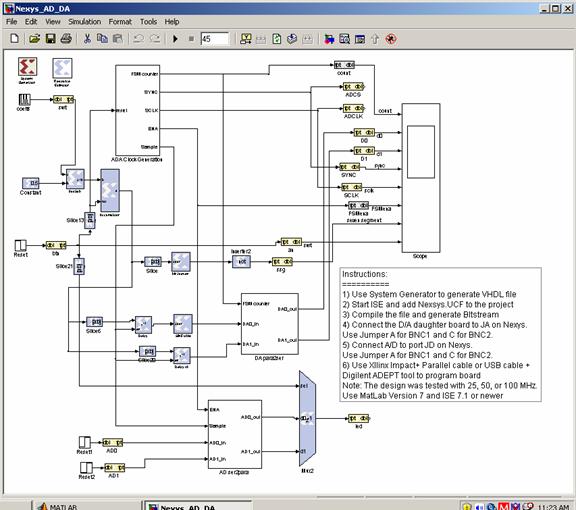
Top level Design
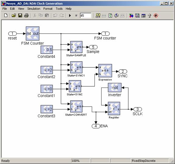
Clock Generation
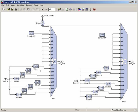
D/A Interface
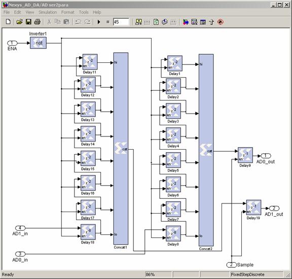
A/D Interface