Team 302: Frequency Multiplier
Datasheets
Challenge Log
| Reference | Date Encountered | Issue | Believed Cause | Purposed Fix | Resolution | Date Resolved | Future Dependants |
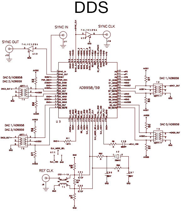
| DDS1 | 11/29/21 | Spurs appearing in a ratio between Ref clk and output frequency | Natural result of DDS chip output Result of Ref clk being below the 200 MHz filter range Registry not being addressed |
Work on output filtering to fix problem Test again with input signal above 10MHz Use Eval Board Software to exam registry values |
Ran the clock at a higher frequency | 12/6/21 | DDS2 DDS3 |
| FIC1 | 1/8/22 | Noise problems with the input signal making rising edges unintelligible by the software | Natural problem that occurs with flip flops and sine waves | Implement a Hysteresis circuit with existing flip flop Purchase a Hysteresis chip to assist the flip flop Use a flip flop with natural hysteresis |
Use a Hysteresis chip and support circuit along with existing flip flop | 1/18/22 | |
| ACS1 | 1/24/22 | Shifting occuring when sending int values to the DDS that have an odd amont of characters in hex | The conversion between the codes integer and the DDS's binary adresses causes an additional 0 to be placed between the first and second least signifigant bit | Instate swith cases for odd and even amounts of hex characters Convert the int values into hex then send the values Alter code to save individual hex characters to be aranged later |
Was only happening in cases with an odd number of outputs, so conditional statements were implemented | 1/28/22 | |
PMC1 DDS2 |
12/16/21 | Evaluation Board has problems outputing signals below 30 kHz | The transformer between the DDS and the filter is not rated low enough to reach levels below that value The DDS itself can not produce clear signals bellow the 15 kHz level |
Remove transformer completely Replace single transformer with seperate isolation and voltage conversion circuits Implement bypass for 30k and lower signals Contact Analog Devices Use Eval Board Software to exam registry values |
Implement a new output stage for the final design that does not incorperate a transformer | 2/15/22 | PCB1 |
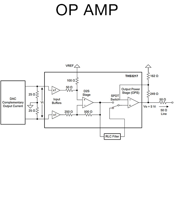
| PMC2 | 1/8/22 | Voltage level at the output is too small to naturally meet spec | Physical property of the DDS with reguards to an input side resistor value | Implement an amplifier circuit when converting from current to voltage driven output Lower the value of the input side resisitor |
Implement a new output stage that uses an amplifier to reach the required spec | 2/15/22 | PCB1 |
| FIC2 | 2/3/22 | Arduino is having trouble reading in signals above 1 MHz | The Arduino ADC is not fast enough to read in the signal | Redesign the circuit for the input circuit Upgrade to a different microproccessor with faster adc Use a filter and rectifier to get a rough but usable input Implement more flip flops and solve the problem in software |
Change to a digital pin which is fast enough as long as the voltage is high enough to trigger | 2/7/22 | |
DDS3 ACS2 |
2/2/22 | Output frequency not syncrhonized with input | Different clocks as signal source | Implement hardware solution utilizing SNK_CLK Implement a software solution utilizing a phase shift command |
Disreguard as this problem does not impact spec nor add signifigant value to warent the man power | 2/16/22 | |
| ACS3 | 2/21/22 | Arduino has troubles connecting to some computers | driver issues | "reinstall driver's on the affect computers | Incorperate a COM selection channel in the computer controls | 3/24/22 | |