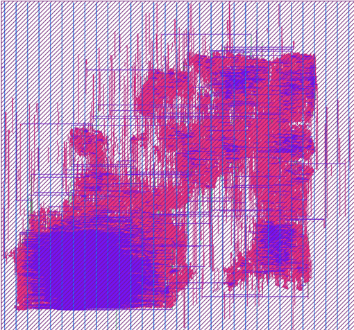
Final Design

Learn about the final design presented during final design day. Also, learn about each individual component that was implemented. Lastly, learn about the future plans of this project

...

ASIC Layout

 The final product is an ASIC design. This design can be seen on the left. This ASIC layout includes the I2C interface, the FFT module, the Tone Detector module, and the control module.
 The plan for this ASIC design is to manufacture it over summer 2023, and the next senior design team through 2023-2024 will receive the ASIC, note its specifications, document any inconsistencies, and test it.

FPGA and MSP430 System

 Since it is very expensive to make personalized integrated circuits, it was decided to model the ASIC design as an FPGA. This system can be seen in the video. The FPGA allows any digital circuits to be created through a Hardware Description Language. The chosen language for the design was Verilog.
 The FPGA and MSP430 design was used as the demonstration for senior design day. The MSP430 captures the audio data at a rate of 5 kHz and converts it to digital data. This digital data is analyzed by the FPGA through the FFT module and the tone detector module determines whether a tone is present. This detected tone is sent to the MSP430 through the I2C module.
 The specifications for the final design is that a tone is detected every 80 ms.

...

FPGA Design

 To model the ASIC before it gets manufactured, it was vital to test the functionaity of the DTMF Detector on an FPGA. These FPGAs have a sea of programmable switches that allows digital circuit to be created from scratch
 With this FPGA, the indevidual components of the design - the I2C interface, the FFT module, the Tone Detector module, and the control module - were designed indevidually, then tested. After all componet testing was concluded, the entire system was tested, producing the final result seen in the design day. The chosen FPGA was the DE1-SoC board.

MSP430FR5994 Launchpad and Educational BoosterPack

 The idea of the project was to produce a purely digital ASIC. In order for the DTMF detector to work, digital data needs to be recieved. Since sound is not digital, a processor needs to capture sound, convert it to a digital signal, and send it to the ASIC for decoding. This is what the MSP430Fr5994 is used for.
 The job of the MSP430FR5994 processor and all of its peripherals connected through the educational boosterpack is to capture sound through the speakers, which outputs an analog signal. This analog signal is given to an analog to digital converter, which outputs a digital signal. This digital signal is given to the ASIC through a communication protocol called I2C
 The on-board microphone has 0 db gain (no gain or attenuation) between the range of dual tone frequnecies interested, the analog to digital converter has a sampling rate of 5 kHz and resolution of 8 bits using a reference of 3.3V. Lastly, the I2C communication runs at 400 kHz.

...

Future Improvements

Improve efficiency of the design: reduce the number of reads and writes through I2C. This will make the design faster than 80 ms per tone because the choke point of the design is the interface between MSP430FR5994 and the FPGA/ASIC

Improve the accuracy of the design: implement a digital filter on the MSP430FR5994 side; this will filter out the noise that is of no interest when detecting dual tones. The sample size of the FFT can also be increased. This will mean each bin of the FFT will correspond to 19.5, instead of 39, giving higher resolution.

Integrate all parts into an ASIC chip: this would mean that Analog to Digital Converters would have to be inserted into the ASIC, therefore, the ASIC would not be fully digital. This would cutoff the interface between the ASIC and MSP430FR5994. This would also make the chip easier to use, as no microcontroller is needed. This is the end goal of the project.